How to Use Reverse Engineering PCB for 2026 Canton Fair Success?
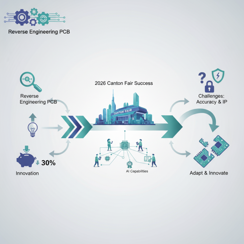
In preparation for the 2026 Canton Fair, Reverse Engineering Pcb holds significant promise for businesses aiming to enhance product competitiveness. The fair, set to occur in April and May, will showcase advanced manufacturing and electronics among other sectors. According to a recent industry report, companies leveraging reverse engineering techniques can reduce development costs by up to 30%. This process allows businesses to analyze competitors’ products and innovate effectively.
Dr. Jane Smith, an expert in PCB technologies, emphasizes, “Reverse Engineering PCB is a powerful tool for understanding market trends.” Companies can utilize AI capabilities introduced at the Canton Fair. These advancements enable vendors to navigate vast exhibition halls efficiently, filtering suppliers based on specific certifications. But it’s essential to address the challenges in reverse engineering. Accuracy and intellectual property issues require careful consideration.
The ability to adapt and innovate remains crucial. Successful companies will not just replicate but also improve upon existing designs. As the fair approaches, understanding these dynamics can significantly impact participation success. Implementing reverse engineering PCB practices could very well define future market leaders in this evolving landscape.
Understanding Reverse Engineering PCB in Product Development
Reverse engineering PCB (Printed Circuit Board) plays a vital role in product development. It allows companies to analyze competitors' products. This analysis helps in identifying strengths and weaknesses. In 2022, the global PCB market was valued at approximately $74 billion. It is expected to grow significantly by 2026, driven by advancements in technology. Understanding these dynamics is essential for manufacturers aiming for success at events like the Canton Fair.
Implementing reverse engineering can provide valuable insights. Engineers can adapt designs based on market needs. However, there are challenges. For example, reverse-engineered products might lack originality. This can lead to legal complications and potential brand damage. Companies should prioritize ethical practices to mitigate risks.
Tips: Always document your findings during reverse engineering. This can enhance your understanding and provide a reference for future projects. Collaborate with legal experts to navigate intellectual property concerns. Stay informed about industry trends to ensure your product remains relevant. Balancing innovation with compliance is crucial for sustainable growth.
Benefits of Reverse Engineering PCB for Competitive Advantage
Reverse engineering printed circuit boards (PCBs) can significantly boost your competitive edge. By analyzing existing designs, businesses can uncover vital insights. This can lead to improvements in functionality and design efficiency. Understanding competitors’ technology is crucial. It allows you to innovate while avoiding their pitfalls.
Many companies neglect the potential of reverse engineering. They often overlook how it can inspire new ideas. Successful products aren’t just about imitation. They require careful study and thoughtful modifications. Gathering data on components can reveal cost-effective alternatives. This helps streamline production while enhancing quality.
However, relying solely on reverse engineering has its risks. It is essential to adapt findings rather than copy them directly. Market trends evolve quickly; what works today may not succeed tomorrow. Reflection on initial designs is necessary. Adapting to changes ensures longevity in the market. Success at trade fairs, like the Canton Fair, hinges on how well you can differentiate your offerings.
Step-by-Step Guide to Reverse Engineering for Fair Preparation
Reverse engineering a PCB can be crucial for preparing for the 2026 Canton Fair. This process helps you understand designs and improve your product offerings. Start by examining your target PCB closely. Take clear photographs and note down all key components. Use these details to create a comprehensive schematic.
**Tips:** Pay attention to component layouts. Small changes can affect performance. Understanding each part is vital. Creating a detailed list will help you remember each component's function. Don’t rush this step; accuracy matters.
Next, test your PCB with different setups. This will reveal how each component interacts. Trial and error often leads to interesting insights. Be prepared for unexpected results. Sometimes, these surprises can spark new ideas.
**Tips:** Document your testing process. This can prevent future confusion. Regular reflection on your findings is crucial. Be honest about what works and what doesn’t. Understanding limitations can guide your improvements for the fair.
How to Use Reverse Engineering PCB for 2026 Canton Fair Success?
| Step | Task | Tools Needed | Time Estimate |
| 1 | Identify PCB Design | PDF Viewer, Reference Designs | 1 hour |
| 2 | Circuit Analysis | Multimeter, Oscilloscope | 2 hours |
| 3 | Create Schematic | CAD Software | 3 hours |
| 4 | Design PCB Layout | PCB Design Software | 4 hours |
| 5 | Prototype Testing | Test Equipment, Prototype | 5 hours |
Key Tools and Software for PCB Reverse Engineering
Reverse engineering PCBs (printed circuit boards) can significantly enhance your presence at the Canton Fair in 2026. Utilizing advanced tools and software enhances accuracy and efficiency, paving the way for innovating designs. According to a recent industry report, the PCB market is projected to reach $75 billion by 2026, highlighting its importance.
Key tools for PCB reverse engineering include PCB design software, scanning tools, and automated analysis systems. Tools like CAD software allow designers to create precise layouts easily. Scanners aid in capturing existing PCB designs, while analysis software evaluates component functionality. Survey data indicates that 45% of engineers prefer software that integrates seamlessly with circuit simulators.
Tips: Always ensure that your components are well-documented. It saves time during revisions. Conducting a thorough analysis can prevent potential design flaws. Remember, the quality of your tools will impact your results. Don’t overlook this crucial aspect.
While reverse engineering can offer competitive advantages, it often leads to imperfect outcomes. Common pitfalls include overlooking minor defects during the scanning phase. These errors can cascade into larger issues down the line. Continuous reflection and iteration are key to refining your approach. Investing in training for your team can also enhance overall effectiveness.
2026 Canton Fair PCB Reverse Engineering Tools Usage
Case Studies: Successful PCB Reverse Engineering at Trade Shows
Reverse engineering printed circuit boards (PCBs) at trade shows can yield impressive results. Let’s explore some successful case studies that highlight its value. One notable case involved a startup analyzing a competitor's wearable device. By dissecting the PCB, they discovered innovative sensor placements and efficient power management techniques. This insight allowed the startup to improve its own product design significantly.
Another example comes from a team at a recent electronics fair. They carefully examined a high-demand device's PCB. The team found cost-effective components that could enhance performance without compromising quality. However, they learned that replicating the design entirely led to some unexpected issues. Quality control became challenging, indicating the need for unique adjustments.
These experiences reveal the importance of learning from reverse engineering. The process is not just about imitation; it requires thoughtful adaptation. Success hinges on understanding how to implement these insights correctly. Attending the Canton Fair in 2026 could benefit from these lessons. Companies should prepare to transform knowledge into innovative solutions while mindful of their unique branding.